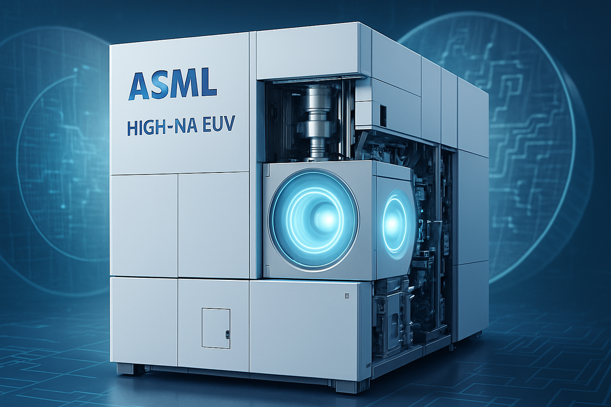
ASML's (AMS: ASML) groundbreaking High-Numerical Aperture (High-NA) Extreme Ultraviolet (EUV) lithography tools, specifically the TWINSCAN EXE:5000 and its successor, the TWINSCAN EXE:5200B, are rapidly becoming the cornerstone of cutting-edge chip manufacturing. These advanced systems are crucial for pushing the boundaries of Moore's Law, enabling the production of semiconductors with features smaller than 2 nanometers. As of September 30, 2025, their deployment marks a pivotal moment, promising to unlock unprecedented transistor densities and performance for the next generation of AI, high-performance computing (HPC), and mobile technologies.
The immediate implication is a significant acceleration in the race for advanced chip leadership. Early adopters like Intel (NASDAQ: INTC) are already leveraging High-NA EUV to simplify complex manufacturing processes, reduce production cycle times, and enhance yields, setting a new benchmark for what's achievable in silicon. However, the staggering cost of these machines, approaching $400 million each, and the intricate integration challenges are leading to varied adoption strategies among other industry giants, hinting at a potentially diversified path forward for leading-edge chip production.
Unpacking the Technological Marvel: ASML's High-NA EUV
ASML's High-NA EUV lithography systems are defined by their increased numerical aperture (NA) of 0.55, a substantial leap from the 0.33 NA of previous EUV generations. This enhancement enables an 8 nm resolution with a single exposure, a marked improvement over the 13 nm resolution of Low-NA EUV systems. This superior resolution allows chipmakers to print features approximately 1.7 times smaller, leading to a nearly threefold increase in transistor density. Such precision is indispensable for manufacturing advanced logic and memory chips, directly enabling the industry's progression to sub-2 nm logic nodes and leading-edge DRAM.
The timeline leading to this moment has been a decade in the making. ASML began developing its High-NA machines around 2016. Intel (NASDAQ: INTC) was the first to commit, placing an order for the TWINSCAN EXE:5000 in 2018 and the more advanced EXE:5200 in 2022. The first modules of the EXE:5000 were shipped to Intel's Oregon facility in December 2023 for R&D, with the full system operational by early 2024. ASML began delivering the newer EXE:5200 model in the second quarter of 2025, primarily to Intel. Samsung (KRX: 005930) reportedly deployed its first High-NA EUV machine (EXE:5000) at its Hwaseong Campus for R&D in March 2025, while TSMC (TPE: 2330) was scheduled to receive its first High-NA EUV equipment (EXE:5000) by the end of September 2024 for R&D. As of September 30, 2025, these initial deployments are primarily for R&D and process development, with limited production use ("phase two") expected around 2026-2027, and full volume manufacturing ("phase three") anticipated later.
Key players and stakeholders in this technological revolution include ASML (AMS: ASML) itself, the sole manufacturer of these systems. ZEISS SMT, a strategic partner, exclusively supplies the advanced optical systems, including the complex mirrors required for High-NA EUV. On the customer side, Intel (NASDAQ: INTC) stands out for its aggressive adoption, aiming to use High-NA for its 14A node expected in 2026. TSMC (TPE: 2330) and Samsung (KRX: 005930) are also critical customers, albeit with more cautious and phased adoption strategies, influenced by the high cost and their existing roadmaps. SK Hynix (KRX: 000660) is also a significant player, planning to integrate High-NA for advanced memory production. Research institutions like Imec (IMEC) play a crucial role in collaborative process development.
Initial market reactions have been a mix of excitement and pragmatism. The industry widely acknowledges High-NA EUV as indispensable for extending Moore's Law and enabling sub-2nm nodes, crucial for the AI era. However, the approximate $380 million price tag per machine represents a significant financial burden, leading to varied adoption timelines. Intel's early feedback has been positive, reporting substantial reductions in process steps and improved wafer processing. Samsung has also noted a 60% reduction in cycle time for certain applications. These early successes underscore the technology's potential, even as chipmakers carefully weigh the immense investment against long-term benefits.
The Winners and Losers in the High-NA EUV Race
The advent of ASML's (AMS: ASML) High-NA EUV lithography tools is creating clear delineations between potential winners and those facing significant challenges in the semiconductor industry. As of September 30, 2025, the ability to access and effectively deploy this technology will largely dictate a company's competitive edge in the advanced chip market.
ASML (AMS: ASML) is the undisputed primary winner. As the sole provider of these critical machines, its market dominance in advanced lithography is further cemented. The company is projected to see a sharp recovery in EUV revenues, with High-NA sales expected to triple in 2025, contributing significantly to its overall growth and solidifying its indispensable role in the global tech ecosystem.
Intel (NASDAQ: INTC) is positioned as a major winner through its aggressive early adoption strategy. By being the first to receive and integrate High-NA EUV, Intel aims to regain process leadership and bolster its foundry services. Its early successes in reducing process steps and increasing wafer output demonstrate a clear path to leveraging this technology for its 14A node, expected in 2026. This move is crucial for Intel's ambition to compete with TSMC (TPE: 2330) and Samsung (KRX: 005930) at the bleeding edge.
SK Hynix (KRX: 000660) is emerging as a significant winner in the memory sector, having assembled the industry's first High-NA EUV lithography system for mass production at its M16 fab. This strategic investment positions the company to produce next-generation DRAM and strengthen its high-value memory product offerings for AI applications, aiming for improved performance and cost competitiveness.
Samsung Electronics (KRX: 005930), despite a more cautious approach than Intel, is also a likely winner. Its plans for commercial High-NA EUV implementation by 2027 for its 1.4nm foundry process, coupled with early positive results in cycle time reduction, indicate a strong commitment to remaining at the forefront of chip manufacturing. Samsung's active collaboration with ecosystem partners further strengthens its position.
The broader semiconductor equipment and materials ecosystem also stands to gain. Companies like Lam Research Corporation (NASDAQ: LRCX) and Applied Materials, Inc. (NASDAQ: AMAT) will benefit from increased demand for complementary etching and deposition equipment, which become even more critical for advanced nodes. KLA Corporation (NASDAQ: KLAC), with its metrology and inspection tools, is indispensable for ensuring yield and quality at these minuscule dimensions. Tokyo Electron Limited (TYO: 8035), JSR Corporation (TYO: 4185), Synopsys, Inc. (NASDAQ: SNPS), and Lasertec Corporation (TYO: 6920) are all poised to win by providing specialized materials, design software, and inspection equipment essential for the High-NA EUV workflow.
Conversely, companies that fail to keep pace will face significant headwinds. Nikon Corporation (TYO: 7731) and Canon Inc. (TYO: 7751), once lithography leaders, are likely to lose further market share in advanced nodes due to their focus on older Deep Ultraviolet (DUV) technologies and lack of meaningful EUV progress. Chinese Semiconductor Manufacturers, such as SMIC (HKG: 0981), face severe challenges due to stringent export controls preventing them from acquiring ASML's advanced EUV tools, effectively locking them out of leading-edge production and widening the technological gap.
TSMC (TPE: 2330), while a long-term leader, could face short-term competitive pressure. Its cautious stance on immediate widespread High-NA EUV adoption for its A14 process, opting to optimize existing Low-NA EUV, might see Intel gain a temporary lead in bleeding-edge process technology. However, TSMC's eventual plans to adopt High-NA for its A14P node indicate a strategic, albeit delayed, engagement.
Ultimately, the successful integration of High-NA EUV will empower companies to capture market share in high-growth segments, enhance profitability through improved yields and efficiency, and define their strategic direction in the AI era. Those unable to adapt will be relegated to less profitable, mature nodes, facing declining market relevance.
Wider Significance: A New Era of Geopolitics and Innovation
The introduction of ASML's (AMS: ASML) High-NA EUV lithography tools extends far beyond mere technological advancement; it represents a profound shift in broader industry trends, geopolitical dynamics, and the very future of digital innovation. As of September 30, 2025, this technology is not just enabling smaller chips, but reshaping global power balances and the competitive landscape.
This development squarely fits into the broader industry trend of hyper-scaling and the relentless pursuit of Moore's Law. High-NA EUV is the linchpin for achieving sub-2nm logic nodes and next-generation memory, which are critical for the insatiable demands of artificial intelligence (AI), 5G, and high-performance computing (HPC). By simplifying multi-patterning and drastically reducing process steps, it promises not only denser chips but also more efficient and cost-effective manufacturing in the long run, despite the high initial investment. The industry is witnessing a phased adoption, with initial R&D deployments in 2025 transitioning to limited production by 2026-2027, highlighting the complexity and strategic importance of this rollout.
The ripple effects on competitors and partners are substantial. ASML's near-monopoly on advanced EUV technology solidifies its indispensable position. However, the differing adoption strategies among leading chipmakers — Intel's (NASDAQ: INTC) aggressive early embrace versus TSMC's (TPE: 2330) and Samsung's (KRX: 005930) more cautious approach – could lead to temporary shifts in competitive advantage. Intel's proactive stance aims to reclaim technological leadership, potentially putting pressure on TSMC to accelerate its High-NA integration. The entire ecosystem, from optical suppliers like ZEISS SMT to metrology and material providers, is intricately linked, with collaborations like IBM's (NYSE: IBM) and SCREEN Semiconductor Solutions' work on cleaning procedures underscoring the extreme precision required.
Regulatory and policy implications are perhaps the most significant non-technical aspect. High-NA EUV is at the epicenter of geopolitical competition, particularly between the U.S. and China. Export controls, primarily driven by the U.S. and implemented by the Dutch government, severely restrict ASML's ability to sell its most advanced tools to China. This has led to a projected 36% fall in ASML's China sales in 2025 and is fueling China's accelerated push for semiconductor self-sufficiency, albeit with a significant technological lag. Conversely, government initiatives like the U.S. CHIPS and Science Act are designed to bolster domestic advanced manufacturing, indirectly supporting the adoption of High-NA EUV by companies like Intel within the U.S. This concentration of critical technology in one company, ASML, also raises global concerns about supply chain security and national technological sovereignty.
Historically, this transition mirrors past shifts in lithography, such as the move from 193nm immersion to Low-NA EUV. Each transition has been driven by the need for higher resolution through shorter wavelengths and increased numerical aperture. The challenges encountered with High-NA EUV—its immense cost, the need for significant fab reconfigurations due to its size, and adjustments to chip designs due to a smaller imaging field—echo the hurdles faced during earlier lithography advancements. However, ASML claims that High-NA EUV is maturing faster than its Low-NA predecessor, indicating lessons learned and a more robust ecosystem. The industry is already looking beyond, with discussions around "Hyper-NA EUV" (0.75 NA) for the early 2030s, signifying a continuous, albeit increasingly challenging, drive for lithographic advancement.
The Road Ahead: Navigating the High-NA Horizon
As ASML's (AMS: ASML) High-NA EUV lithography tools move from initial deployment to broader integration, the semiconductor industry stands at a critical juncture. The path forward, both in the short and long term, will be shaped by technological readiness, economic realities, and geopolitical currents.
In the short term (next 1-2 years, 2025-2026), the primary focus will remain on the successful integration and optimization of High-NA EUV systems by early adopters. Intel (NASDAQ: INTC) will be a key bellwether, demonstrating the technology's capabilities for its 18A and 14A nodes. ASML aims to ship at least five High-NA EUV systems in 2025, with sales projected to triple. We can expect continued R&D efforts from TSMC (TPE: 2330) and Samsung (KRX: 005930), with limited production use ("phase two") of High-NA EUV anticipated around 2026-2027. The immediate challenge will be for chipmakers to rapidly adapt their design rules and process flows to fully leverage the benefits of High-NA, particularly its ability to simplify multi-patterning and reduce manufacturing steps.
Looking at the long term (3-5+ years, 2027-2030 and beyond), High-NA EUV is set to become the foundational technology for scaling chips beyond 2nm, targeting 1.5nm and sub-1nm processes. ASML expects volume manufacturing adoption to begin after 2027, with Intel aiming for risk production on its 14A process in 2027 and volume production by 2028. This will be critical for sustaining the exponential growth of AI and HPC. Beyond High-NA, ASML is already exploring "Hyper-NA" EUV, with a numerical aperture of ~0.75, for deployment around 2030-2035, indicating a relentless pursuit of miniaturization. However, the role of High-NA EUV in DRAM production might evolve, with some memory makers reportedly delaying adoption due to high costs and potential shifts towards 3D DRAM architectures that may not require EUV for certain processes.
Strategic pivots or adaptations will be crucial for all stakeholders. Chipmakers will need to manage the immense capital expenditure of High-NA tools while optimizing their existing Low-NA EUV capabilities. The shift towards new transistor architectures like Gate-All-Around FET (GAAFET) and Complementary FET (CFET) could also lead to a greater emphasis on advanced etching technologies, requiring adaptations in overall manufacturing strategies. ASML, for its part, is investing heavily in holistic lithography solutions, integrating its systems with computational lithography software and metrology tools. Its strategic investment in AI, exemplified by its stake in Mistral AI, signals an adaptation to leverage AI across its product portfolio for enhanced R&D and operational efficiency. ASML also aims to ramp up its manufacturing capacity for High-NA EUV tools to 20 units annually by 2027/2028.
Market opportunities are vast, primarily driven by the insatiable demand for advanced AI processors and HPC chips. High-NA EUV will enable new frontiers in robotics, augmented reality, and the Internet of Things. ASML's dominant market position ensures it remains at the heart of this growth. However, challenges persist, including the exorbitant cost of the machines, which could slow adoption for some. Technical complexities in achieving high yields for early High-NA processes, such as Samsung's Exynos 2600 facing low yields, need to be overcome. Geopolitical factors and export controls, particularly impacting sales to China, remain a significant headwind, potentially leading to bifurcated supply chains. Macroeconomic uncertainties could also lead to slower-than-expected capital spending.
Potential scenarios range from successful widespread adoption leading to rapid industry acceleration (most likely) to a slower-than-expected ramp-up due to cost and technical hurdles. A third scenario involves a strategic re-evaluation where High-NA EUV becomes critical for logic but its role in memory might diminish, or where etching gains relatively more importance for certain advanced architectures. Finally, geopolitical disruptions remain an ongoing risk, potentially impacting ASML's market access and global technological progression.
Comprehensive Wrap-up: The Indispensable Enabler
ASML's (AMS: ASML) High-NA EUV lithography tools are not merely incremental upgrades; they are indispensable enablers for the next chapter of semiconductor innovation. As of September 30, 2025, the industry is witnessing the dawn of a new era, characterized by unprecedented chip densities and performance, primarily driven by these advanced machines.
Key takeaways from recent developments underscore the positive early performance of High-NA EUV, with leading chipmakers like Intel (NASDAQ: INTC) reporting significant reductions in process steps and improved wafer processing. Samsung (KRX: 005930) has also noted substantial cycle time reductions. These early successes, coupled with ASML's robust financial projections for High-NA sales tripling in 2025, signal strong validation of the technology's potential.
The market moving forward will be defined by a dual dynamic: the immense opportunity presented by AI and HPC, and the inherent challenges of integrating such complex and expensive technology. High-NA EUV is critical for scaling to 2nm and beyond, solidifying ASML's near-monopoly. However, the high cost is prompting a cautious, phased adoption by some, notably TSMC (TPE: 2330) for certain nodes, potentially extending the life of current EUV systems. Geopolitical headwinds, particularly export restrictions to China, continue to influence market dynamics and ASML's revenue streams.
The lasting significance and impact of High-NA EUV are profound. It ensures the continued progression of Moore's Law, enabling the miniaturization and performance enhancements essential for future technological advancements across all sectors. By simplifying manufacturing processes and boosting efficiency, it promises long-term cost benefits for chipmakers. ASML's continuous innovation, including the exploration of "Hyper-NA EUV," reinforces its role as the central pillar of advanced chipmaking.
Investors should watch for several key indicators in the coming months. Firstly, monitor the pace of new High-NA EUV orders and actual deliveries, particularly from customers beyond Intel, to gauge broader market adoption. Secondly, pay close attention to statements from major foundries regarding their deployment timelines and any shifts in strategy due to cost or architectural changes. ASML's guidance for 2026 will be crucial, as macroeconomic uncertainties could influence capital spending. Gross margins, geopolitical developments (especially regarding China), and any advancements in alternative chipmaking technologies also warrant close scrutiny.
In essence, ASML's High-NA EUV technology positions the company and its leading customers for significant growth and technological leadership in the years to come. While navigating the complexities of cost, integration, and geopolitics, the long-term trajectory for advanced semiconductor innovation remains firmly in the hands of these cutting-edge lithography tools.
This content is intended for informational purposes only and is not financial advice.