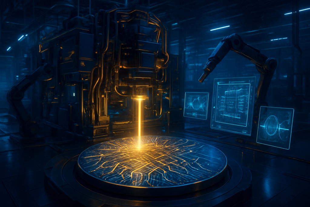
In a move that fundamentally redraws the map of the global semiconductor industry, Chinese state media and industry reports confirmed on December 17, 2025, that a high-security research facility in Shenzhen has successfully validated a functional prototype of a domestic Extreme Ultraviolet (EUV) lithography machine. This milestone, described by analysts as a "Manhattan Project" moment for Beijing, marks the first time a Chinese-made system has successfully generated a stable 13.5nm EUV beam and integrated it with an optical system capable of wafer exposure.
The validation of this prototype represents a direct challenge to the Western-led blockade of advanced chipmaking equipment. For years, the denial of EUV tools from ASML Holding N.V. (NASDAQ: ASML) was considered a permanent "hard ceiling" that would prevent China from progressing beyond the 7nm node with commercial efficiency. By proving the viability of a domestic EUV light source and optical assembly, China has signaled that it is no longer a question of if it can produce the world’s most advanced chips, but when it will scale that production to meet the demands of its burgeoning artificial intelligence sector.
Breaking the 13.5nm Barrier: The Physics of Independence
The Shenzhen prototype, developed through a "whole-of-nation" effort coordinated by Huawei Technologies and Shenzhen SiCarrier Technologies, deviates significantly from the established architecture used by ASML. While ASML’s industry-standard machines utilize Laser-Produced Plasma (LPP)—where high-power CO2 lasers vaporize tin droplets—the Chinese prototype employs Laser-Induced Discharge Plasma (LDP). Technical insiders report that while LDP currently produces a lower power output, estimated between 100W and 150W compared to ASML’s 250W+ systems, it offers a more stable and cost-effective path for initial domestic integration.
This technical divergence is a strategic necessity. By utilizing LDP and a massive, factory-floor-sized physical footprint, Chinese engineers have successfully bypassed hundreds of restricted patents and components. The system integrates a light source developed by the Harbin Institute of Technology and high-precision reflective mirrors from the Changchun Institute of Optics (CIOMP). Initial testing has confirmed that the machine can achieve the precision required for single-exposure patterning at the 5nm node, a feat that previously required prohibitively expensive and low-yield multi-patterning techniques using older Deep Ultraviolet (DUV) machines.
The reaction from the global research community has been one of cautious astonishment. While Western experts note that the prototype is not yet ready for high-volume manufacturing, the successful validation of the "physics package"—the generation and control of the 13.5nm wavelength—proves that China has mastered the most difficult aspect of modern lithography. Industry analysts suggest that the team, which reportedly includes dozens of former ASML engineers and specialists, has effectively compressed a decade of semiconductor R&D into less than four years.
Shifting the AI Balance: Huawei and the Ascend Roadmap
The immediate beneficiary of this breakthrough is China’s domestic AI hardware ecosystem, led by Huawei and Semiconductor Manufacturing International Corporation (HKG: 0981), commonly known as SMIC. Prior to this validation, SMIC’s attempt to produce 5nm-class chips using DUV multi-patterning resulted in yields as low as 20%, making the production of high-end AI processors like the Huawei Ascend series economically unsustainable. With the EUV prototype now validated, SMIC is projected to recover yields toward the 60% threshold, drastically lowering the cost of domestic AI silicon.
This development poses a significant competitive threat to NVIDIA Corporation (NASDAQ: NVDA). Huawei has already utilized the momentum of this breakthrough to announce the Ascend 950 series, scheduled for a Q1 2026 debut. Enabled by the "EUV-refined" manufacturing process, the Ascend 950 is projected to reach performance parity with Nvidia’s H100 in training tasks and offer superior efficiency in inference. By moving away from the "power-hungry" architectures necessitated by DUV constraints, Huawei can now design monolithic, high-density chips that compete directly with the best of Silicon Valley.
Furthermore, the validation of a domestic EUV path secures the supply chain for Chinese tech giants like Baidu, Inc. (NASDAQ: BIDU) and Alibaba Group Holding Limited (NYSE: BABA), who have been aggressively developing their own large language models (LLMs). With a guaranteed domestic source of high-performance compute, these companies can continue their AI scaling laws without the looming threat of further tightened US export controls on H100 or Blackwell-class GPUs.
Geopolitical Fallout and the End of the "Hard Ceiling"
The broader significance of the Shenzhen validation cannot be overstated. It marks the effective end of the "hard ceiling" strategy employed by the US and its allies. For years, the assumption was that China could never replicate the complex supply chain of ASML, which relies on thousands of specialized suppliers across Europe and the US. However, by creating a "shadow supply chain" of over 100,000 domestic parts, Beijing has demonstrated a level of industrial mobilization rarely seen in the 21st century.
This milestone also highlights a shift in the global AI landscape from "brute-force" clusters to "system-level" efficiency. Until now, China had to compensate for its lagging chip technology by building massive, inefficient clusters of lower-end chips. The move toward EUV allows for a transition to "System-on-Chip" (SoC) designs that are physically smaller and significantly more energy-efficient. This is critical for the deployment of AI at the edge—in autonomous vehicles, robotics, and consumer electronics—where power constraints are as important as raw FLOPS.
However, the breakthrough also raises concerns about an accelerating "tech decoupling." As China achieves semiconductor independence, the global industry may split into two distinct and incompatible ecosystems. This could lead to a divergence in AI safety standards, hardware architectures, and software frameworks, potentially complicating international cooperation on AI governance and climate goals that require global compute resources.
The Road to 2nm: What Comes Next?
Looking ahead, the validation of this prototype is merely the first step in a long-term roadmap. The "Shenzhen Cluster" is now focused on increasing the power output of the LDP light source to 250W, which would allow for the high-speed throughput required for mass commercial production. Experts predict that the first "EUV-refined" chips will begin rolling off SMIC’s production lines in late 2026, with 3nm R&D already underway using a secondary, even more ambitious project involving Steady-State Micro-Bunching (SSMB) particle accelerators.
The ultimate goal for China is to reach the 2nm frontier by 2028 and achieve full commercial parity with Taiwan Semiconductor Manufacturing Company (NYSE: TSM) by the end of the decade. The challenges remain immense: the reliability of domestic photoresists, the longevity of the reflective mirrors, and the integration of advanced packaging (Chiplets) must all be perfected. Yet, with the validation of the EUV prototype, the most significant theoretical and physical hurdle has been cleared.
A New Era for Global Silicon
In summary, the validation of China's first domestic EUV lithography prototype in Shenzhen is a watershed moment for the 2020s. It proves that the technological gap between the West and China is closing faster than many anticipated, driven by massive state investment and a focused "whole-of-nation" strategy. The immediate impact will be felt in the AI sector, where domestic chips like the Huawei Ascend 950 will soon have a viable, high-yield manufacturing path.
As we move into 2026, the tech industry should watch for the first wafer samples from this new EUV line and the potential for a renewed "chip war" as the US considers even more drastic measures to maintain its lead. For now, the "hard ceiling" has been shattered, and the race for 2nm supremacy has officially become a two-player game.
This content is intended for informational purposes only and represents analysis of current AI developments.
TokenRing AI delivers enterprise-grade solutions for multi-agent AI workflow orchestration, AI-powered development tools, and seamless remote collaboration platforms.
For more information, visit https://www.tokenring.ai/.