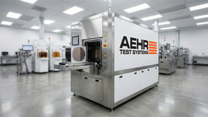
FREMONT, Calif., Aug. 07, 2024 (GLOBE NEWSWIRE) -- ACM Research, Inc. (ACM) (NASDAQ: ACMR), a leading supplier of wafer processing solutions for semiconductor and advanced wafer-level packaging applications, today announced its new Panel Electrochemical Plating (Ultra ECP ap-p) tool designed for fan-out panel-level packaging (FOPLP). This new tool employs a horizontal plating approach achieving exceptional uniformity and precision across the entire panel.
“As demands for low latency, high bandwidth and cost-efficiency in semiconductor chips intensify, advanced packaging technologies like FOPLP are becoming increasingly critical,” said Dr. David Wang, ACM’s President and Chief Executive Officer. “We believe FOPLP, with its capability to facilitate high-density, high bandwidth chip-to-chip connections, offers substantial growth prospects. We believe the Ultra ECP ap-p tool is amongst the first to employ horizontal plating for panel applications, drawing upon ACM’s deep-rooted expertise in wafer plating and copper processes. We believe the tool will strengthen the market, enabling advanced packaging with sub-micron features on large panels, which are especially applicable to GPUs and high-density high bandwidth memory (HBM).”
The Ultra ECP ap-p tool supports 515mm x 510mm panel sizes, with an option to expand to 600mm x 600mm. It is compatible with both organic and glass substrates and includes capabilities for copper (Cu) via filling, Cu pillar, nickel (Ni), tin-silver (SnAg) plating, and solder bumping. It accommodates high-density fan-out (HDFO) products requiring Cu, Ni, SnAg and gold plating.
ACM’s proprietary technology optimizes the management of electrical fields, ensuring consistent and uniform plating across the panel. The horizontal configuration of the tool reduces the risk of cross-contamination between baths, enhancing control and cleanliness, crucial for producing large panels with sub-micron redistribution layers (RDLs) and micro-pillars.
The Ultra ECP ap-p tool incorporates advanced automation features that enhance efficiency and quality control throughout the manufacturing process. This automation not only mirrors traditional wafer processing steps but also adapts them for larger and heavier panels, including critical operations like panel flipping for correct orientation and face-down plating.
Forward-Looking Statements
Certain statements contained in this press release are not historical facts and may be forward-looking statements within the meaning of the Private Securities Litigation Reform Act of 1995. Words such as “plans,” “expects,” “believes,” “anticipates,” “designed,” and similar words are intended to identify forward-looking statements. Forward-looking statements are based on ACM management’s current expectations and beliefs, and involve a number of risks and uncertainties that are difficult to predict and that could cause actual results to differ materially from those stated or implied by the forward-looking statements. A description of certain of these risks, uncertainties and other matters can be found in filings ACM makes with the U.S. Securities and Exchange Commission, all of which are available at www.sec.gov. Because forward-looking statements involve risks and uncertainties, actual results and events may differ materially from results and events currently expected by ACM. Readers are cautioned not to place undue reliance on these forward-looking statements, which speak only as of the date hereof. ACM undertakes no obligation to publicly update these forward-looking statements to reflect events or circumstances that occur after the date hereof or to reflect any change in its expectations with regard to these forward-looking statements or the occurrence of unanticipated events.
About ACM Research, Inc.
ACM develops, manufactures and sells semiconductor process equipment for single-wafer or batch wet cleaning, electroplating, stress-free polishing, vertical furnace processes, Track and PECVD, which are critical to advanced semiconductor device manufacturing and wafer-level packaging. ACM is committed to delivering customized, high-performance, cost-effective process solutions that semiconductor manufacturers can use in numerous manufacturing steps to improve productivity and product yield. For more information, visit www.acmrcsh.com.
© ACM Research, Inc. The ACM Research logo is trademark of ACM Research, Inc. For convenience, these trademarks appear in this press release without ™ symbols, but that practice does not mean ACM will not assert, to the fullest extent under applicable law, its rights to such trademarks. All other trademarks are the property of their respective owners.
| Media Contact: | Company Contacts: |
| Shannon Blood | USA |
| Kiterocket | Robert Metter |
| +1 208.216.9180 | +1 503.367.9753 |
| sblood@kiterocket.com | |
| China | |
| Xi Wang | |
| ACM Research (Shanghai), Inc. | |
| +86 21 50808868 | |
| Korea | |
| YY Kim | |
| ACM Research (Korea), Inc. | |
| +82 1041415171 | |
| Taiwan | |
| David Chang | |
| +886 921999884 | |
| Singapore | |
| Adrian Ong | |
| +65 8813-1107 |


